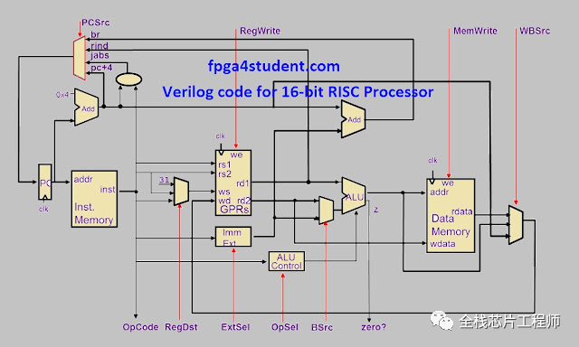
本CPU设计基于16bit RISC指令集、哈佛结构完成,架构图如下:
CPU架构
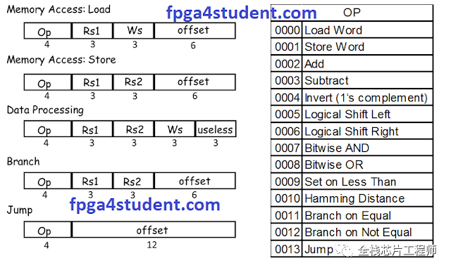
A. Memory Access Instructions1. Load Word:
LD ws, offset(rs1) ws:=Mem16[rs1 + offset]2. Store Word:
ST rs2, offset(rs1) Mem16[rs1 + offset]=rs2
B. Data Processing Instructions1. Add:
ADD ws, rs1, rs2 ws:=rs1 + rs22. Subtract:
SUB ws, rs1, rs2 ws:=rs1 – rs23. Invert (1‘s complement):
INV ws, rs1 ws:=!rs14. Logical Shift Left:
LSL ws, rs1, rs2 ws:=rs1 << rs25. Logical Shift Right:
LSR ws, rs1, rs2 ws:=rs1 >> rs26. Bitwise AND:
AND ws, rs1, rs2 ws:=rs1 • rs27. Bitwise OR:
OR ws, rs1, rs2 ws:=rs1 | rs2
8. Set on Less Than:
SLT ws, rs1, rs2 ws:=1 if rs1 < rs2; ws:=0 if rs1 ≥ rs2C. Control Flow Instructions
1. Branch on Equal:
BEQ rs1, rs2, offset
Branch to (PC + 2 + (offset << 1)) when rs1 = rs22. Branch on Not Equal:
BNE rs1, rs2, offset
Branch to (PC + 2 + (offset << 1)) when rs1 != rs2 3. Jump: JMP offset Jump to {PC [15:13], (offset << 1)}Instruction Format of the RISC

ALU Control Unit Design:

Verilog code for the RISC processor:
1. Verilog code for Instruction Memory :`include “Parameter.v”// fpga4student.com // FPGA projects, VHDL projects, Verilog projects // Verilog code for RISC Processor // Verilog code for Instruction Memorymodule Instruction_Memory( input[15:0] pc, output[15:0] instruction); reg [`col – 1:0] memory [`row_i – 1:0]; wire [3 : 0] rom_addr = pc[4 : 1]; initial begin $readmemb(“./test/test.prog”, memory,0,14); end assign instruction = memory[rom_addr]; endmodule2. Verilog code for register file:`timescale 1ns / 1ps// fpga4student.com // FPGA projects, VHDL projects, Verilog projects // Verilog code for RISC Processor // Verilog code for register filemodule GPRs( input clk, // write port input reg_write_en, input [2:0] reg_write_dest, input [15:0] reg_write_data, //read port 1 input [2:0] reg_read_addr_1, output [15:0] reg_read_data_1, //read port 2 input [2:0] reg_read_addr_2, output [15:0] reg_read_data_2); reg [15:0] reg_array [7:0]; integer i; // write port //reg [2:0] i; initial begin for(i=0;i<8;i=i+1) reg_array[i] <= 16d0; end always @ (posedge clk ) begin if(reg_write_en) begin reg_array[reg_write_dest] <= reg_write_data; end end assign reg_read_data_1 = reg_array[reg_read_addr_1]; assign reg_read_data_2 = reg_array[reg_read_addr_2];endmodule3. Verilog code for Data Memory:`include “Parameter.v”// fpga4student.com // FPGA projects, VHDL projects, Verilog projects // Verilog code for RISC Processor // Verilog code for data Memorymodule Data_Memory( input clk, // address input, shared by read and write port input [15:0] mem_access_addr, // write port input [15:0] mem_write_data, input mem_write_en, input mem_read, // read port output [15:0] mem_read_data);reg [`col – 1:0] memory [`row_d – 1:0];integer f;wire [2:0] ram_addr=mem_access_addr[2:0];initial begin $readmemb(“./test/test.data”, memory); f = $fopen(`filename); $fmonitor(f, “time = %d\n”, $time, “\tmemory[0] = %b\n”, memory[0], “\tmemory[1] = %b\n”, memory[1], “\tmemory[2] = %b\n”, memory[2], “\tmemory[3] = %b\n”, memory[3], “\tmemory[4] = %b\n”, memory[4], “\tmemory[5] = %b\n”, memory[5], “\tmemory[6] = %b\n”, memory[6], “\tmemory[7] = %b\n”, memory[7]); `simulation_time; $fclose(f); end always @(posedge clk) begin if (mem_write_en) memory[ram_addr] <= mem_write_data; end assign mem_read_data = (mem_read==1b1) ? memory[ram_addr]: 16d0;endmodule4. Verilog code for ALU unit:// fpga4student.com // FPGA projects, VHDL projects, Verilog projects // Verilog code for RISC Processor // Verilog code for ALUmodule ALU( input [15:0] a, //src1 input [15:0] b, //src2 input [2:0] alu_control, //function sel output reg [15:0] result, //result output zero );always @(*)begin case(alu_control) 3b000: result = a + b; // add 3b001: result = a – b; // sub 3b010: result = ~a; 3b011: result = a< 3b100: result = a>>b; 3b101: result = a & b; // and 3b110: result = a | b; // or 3b111: begin if (a// fpga4student.com // FPGA projects, VHDL projects, Verilog projects // Verilog code for RISC Processor // Verilog testbench code to test the processormodule test_Risc_16_bit; // Inputs reg clk; // Instantiate the Unit Under Test (UUT) Risc_16_bit uut ( .clk(clk) ); initial begin clk <=0; `simulation_time; $finish; end always begin #5 clk = ~clk; endendmoduleParameter file:`ifndef PARAMETER_H_`define PARAMETER_H_// fpga4student.com // FPGA projects, VHDL projects, Verilog projects // Verilog code for RISC Processor // Parameter file`define col 16 // 16 bits instruction memory, data memory`define row_i 15 // instruction memory, instructions number, this number can be changed. Adding more instructions to verify your design is a good idea.`define row_d 8 // The number of data in data memory. We only use 8 data. Do not change this number. You can change the value of each data inside test.data file. Total number is fixed at 8. `define filename “./test/50001111_50001212.o”`define simulation_time #160`endiftest.prog (Intruction memory)
Example instruction memory file: 0000_0100_0000_0000 // load R0 <- Mem(R2 + 0)0000_0100_0100_0001 // load R1 <- Mem(R2 + 1)0010_0000_0101_0000 // Add R2 <- R0 + R10001_0010_1000_0000 // Store Mem(R1 + 0) <- R20011_0000_0101_0000 // sub R2 <- R0 – R10100_0000_0101_0000 // invert R2 <- !R0 0101_0000_0101_0000 // logical shift left R2 <- R0<0110_0000_0101_0000 // logical shift right R2 <- R0>>R1 0111_0000_0101_0000 // AND R2<- R0 AND R1 1000_0000_0101_0000 // OR R2<- R0 OR R1 1001_0000_0101_0000 // SLT R2 <- 1 if R0 < R1 0010_0000_0000_0000 // Add R0 <- R0 + R01011_0000_0100_0001 // BEQ branch to jump if R0=R1, PCnew= PC+2+offset<<1 = 28 => offset = 11100_0000_0100_0000 // BNE branch to jump if R0!=R1, PCnew= PC+2+offset<<1 = 28 => offset = 01101_0000_0000_0000 // J jump to the beginning addresstest.data (Initial content of data memory)
Example data memory file:0000_0000_0000_00010000_0000_0000_00100000_0000_0000_00010000_0000_0000_00100000_0000_0000_00010000_0000_0000_00100000_0000_0000_00010000_0000_0000_0010感谢阅读,别走!点赞、关注、转发后再走吧

参考链接:
https://www.fpga4student.com/2017/01/verilog-code-for-single-cycle-MIPS-processor.html
https://www.fpga4student.com/2017/04/verilog-code-for-16-bit-risc-processor.html
转载:全栈芯片工程师
免责声明:文章内容来自互联网,本站不对其真实性负责,也不承担任何法律责任,如有侵权等情况,请与本站联系删除。
转载请注明出处:【MCU】16bit CPU设计实战(二)-16位mcu系列芯片有哪些类型 https://www.yhzz.com.cn/a/10488.html