Tap cells●Tap cells are used to provide substrate connection.●They are used to avoid latch-up.●They connect n-well to VDD and p-sub to VSS.●They are inserted in layout at regular intervals based on tap rules (tap to gate distance) defined in the technology DRC file.Filler cells●Filler cells are used to provide rail continuity, thereby reducing the DRC violations created by the base.●Filler cells are designed in such a way that they contain n-well and p substrate.Metal eco-able cells● The filler cells which are converted to attain any functionality are called metal eco-able cells.●The base layers of both filler cells and metal eco-able cells are same. Some extra metal connections will be added in metal eco-able cells to attain the functionality.●Sizes of these cells are more when compared to normal cells of same functionality.●For example, consider a design having hold violation after the fabrication. One way to overcome the violation is to delay the data-path. In this case we can convert metal eco-able cells to buffer for the delay. (generally done during re-spin of chip).Antenna diode●During fabrication stray charges get accumulated in metal layers. The gate gets ruptured when the amount of these charges are more than threshold. This effect is called antenna effect. The threshold is decided by metal layer area to gate area ratio.●To overcome the antenna effect we use antenna diodes.●Zener diodes will be connected to the metal layers to remove the excess charges.
Fig4: Antenna diode●Another way to overcome antenna effect is to add jumpers. Use higher metal layers for connection.
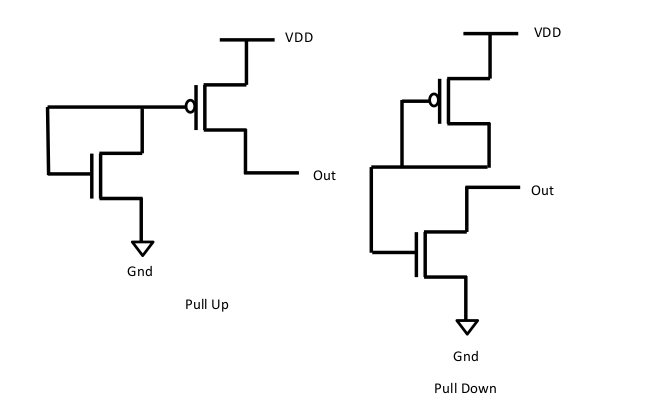
Fig5: JumperDe cap cells (Decoupling capacitor cells)●De cap cells are capacitors added in design between power and ground rails.●When there is drop in power rail, these cells act like a battery and maintain the voltage across rails.●These cells aids IR drop issue and removes glitches in power.●In a design most of the power consumption is done by clock circuits. Assume that all the clock blocks are clustered in an area, then they will consume more power, i.e. they drew more current which will increase IR drop. In this case de cap cells can be used.End cap cell●End cap cells are added near the end of rows to terminate the rows properly.●The n-wells of end cap cells are properly terminated within the cell.Tie cell●Tie cells are used to avoid direct gate connection to the power or ground network thereby protecting the cell from damage.●In your design, some cell inputs may require a logic 0 or logic 1 value. Instead of connecting these to the VDD/VSS rails/rings, you connect them to special cells available in your library called TIE cells.●In tie high cell, nmos acts as diode connected and gives logic 0 to the gate of pmos, so we will get logic 1 as output whereas in tie low cell, pmos act as diode connected and gives logic 1 to the gate of nmos, so we will get logic 0 as output.
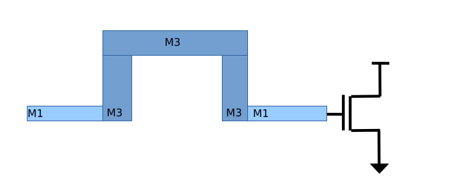
Fig6: Tie cellSpare cell●Spare cells are normal standard cells but they act as redundant cells as they are evenly distributed on the chip in anticipation of future ECO i.e, after the tape out.●After the tape out, sometimes we may have to make some changes to the design to resolve a bug. In these cases we use the pre existing spare cells in the design.●If we carry out the design changes with minimal layer changes, it will save a lot of cost from fabrication point of view as each mask layer has significant cost of its own.●Spare cell inputs are connected to VDD/GND when they are placed in the design and their outputs are left floating.●If they are required to be used, then their inputs are disconnected from VDD/GND and connected to functional logic in ECO mode.
Fig7: Spare CellCharacterization●Characterization is the generation of .lib files, done with respect to PVT corners.●Typically characterization is done for six different loads and six different transitions(slew)●Models used to generate .lib files are NLDM and CCS. CCS is more accurate when compared to NLDM.